|
When you think about materials used by the electronics industry, silicon may be the first one that comes to your mind. The use of silicon in the electronics industry up to this point has been integral to getting the technologies we have now that seemed impossible just a decade ago. The computer chips—also called integrated circuits—have gotten faster as the size of transistors has decreased, allowing the amount of transistors in an integrated circuit to double roughly every two years. This phenomenon was described in Gordon Moore’s 1965 paper Cramming More Components onto Integrated Circuits. 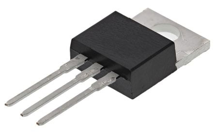 Today, millions of transistors make up the microprocessors found in electronics, each transistor functioning as a simple on/off switch to transmit the ones and zeros that make up electronic data. However, for the better part of a decade, the continued use of silicon as the main component of transistors revealed the limits of the material. Regardless of how many transistors are formed in the microchip, they will operate in the same way: current flows between the "source" terminal and the "drain" terminal, and the flowing switch is controlled by a third terminal called the "gate". . For proper operation, the "gate" must be separated from the other two terminals by a silicon dioxide insulating film. Keeping the "gate" from current is becoming more and more difficult due to the rapid shrinkage of the transistor. The silicon dioxide insulating layer, called dielectric, is only a few atoms thick, and there is no more insulating space on the integrated circuit. This is a problem because thin barriers cannot be effectively isolated, so the chip heats up and loses efficiency. Is there a material better than silicon? 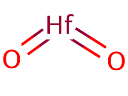 Try hafnium oxide. Back in 2007, IBM and Intel announced that they would begin producing the next-generation computer chips that were smaller and faster than silicon by using hafnium oxide.
Hafnium oxide is a stable, inorganic compound that is a much more effective dielectric than silicon. According to Paul McIntyre from the Stanford University Engineering and Science Institute, California, “Researchers have learnt to deposit very thin films of hafnium oxide and mix it with silica or silicon nitride at the molecular scale to tailor their insulating and charge storage properties.” In addition to replacing silicon in transistors, in 2012, scientists at the University of Cambridge developed a manufacturing process that created hafnium oxide that has the benefit of being a room-temperature, high-deposition rate process. This makes the deployment of hafnium oxide-based electronics, which includes solar cells and semiconductors, along with microchips, much more efficient. The rapid pace of electric development has required the industry to move away from silicon to make its ever-shrinking capacitors. Hafnium oxide is a stepping stone towards more innovation, ensuring the future progress of faster, smarter computers. For more information, please visit https://www.sputtertargets.net/.
28 评论
|
 RSS订阅
RSS订阅
