|
Tungsten sputtering targets are the unsung heroes of the electronics and semiconductor industries, enabling the production of cutting-edge devices that power our modern world. These targets play a crucial role in the thin film deposition process, a fundamental technique in semiconductor manufacturing, OLED production, and more. But what goes into making these high-purity tungsten sputtering targets, and why are they so essential? Let's take a closer look behind the scenes. The Quest for Purity Tungsten, a heavy and dense metal with exceptional thermal and electrical conductivity properties, is the material of choice for sputtering targets. However, not all tungsten is created equal. The semiconductor and electronics industries demand the highest levels of purity to ensure the reliability and performance of their devices. The manufacturing process begins with sourcing raw tungsten materials, typically in the form of tungsten oxides or powders. These raw materials undergo a series of complex chemical and metallurgical processes to extract and refine the tungsten into high-purity metal. Impurities, even in trace amounts, can significantly impact the quality of the sputtering process and the final product. 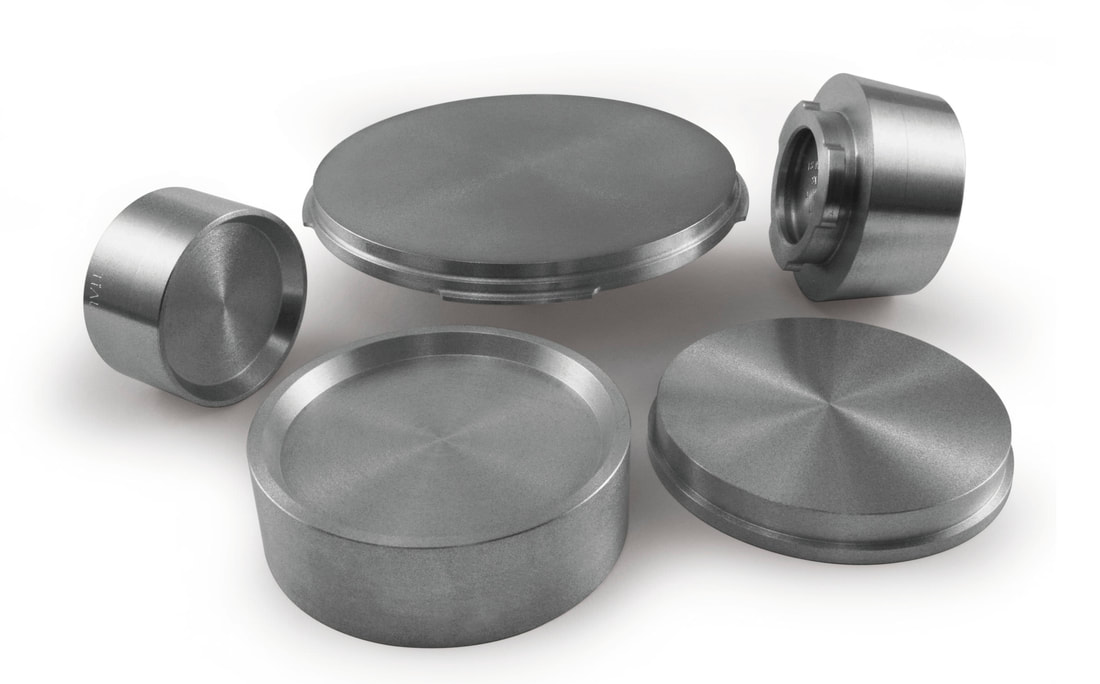 Powder Metallurgy and Forming
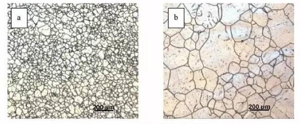
Once the tungsten metal achieves the required level of purity, it is transformed into sputtering targets through a process known as powder metallurgy. In this process, the tungsten powder is carefully blended with a binding agent to create a homogenous mixture. This mixture is then pressed into the desired shape, typically a cylindrical or planar target. The pressing stage is critical for achieving the right density and uniformity. The formed targets must have a precise thickness, ensuring even sputtering during the deposition process. Achieving this level of precision requires expertise and state-of-the-art equipment. Sintering and Thermal Treatment After forming, the tungsten targets undergo sintering, a high-temperature process that fuses the tungsten particles together. This step enhances the mechanical strength of the target and further eliminates any remaining impurities. Sintering can occur in a vacuum or hydrogen atmosphere to prevent contamination. Following sintering, the targets may undergo additional thermal treatments to optimize their microstructure. These treatments help ensure the targets can withstand the rigorous conditions of the sputtering process, which involves bombarding the target material with high-energy ions to dislodge atoms for deposition onto substrates. Quality Control and Testing Quality control is paramount throughout the manufacturing process. Advanced techniques such as X-ray diffraction and spectroscopy are employed to analyze the target's composition and crystal structure. These tests ensure that the final product meets the stringent purity and quality standards required by the semiconductor and electronics industries. Customization and Innovation While the basics of tungsten sputtering target manufacturing remain consistent, innovation continues to drive the industry forward. Research and development efforts focus on refining the manufacturing processes, exploring new materials and coatings, and optimizing target designs to enhance performance and longevity. Conclusion Tungsten sputtering targets are a testament to precision engineering and materials science. Behind the scenes, these high-purity targets undergo a rigorous journey from raw materials to the finished product, with each step carefully controlled and monitored. Their exceptional purity, density, and uniformity make them indispensable tools in the production of semiconductor devices, OLED screens, and a wide range of other electronic components. As technology continues to advance, the manufacturing of tungsten sputtering targets will undoubtedly play a pivotal role in shaping the future of electronics and semiconductor industries. For more information, please visit sputtertargets.net.
0 评论
When you think about materials used by the electronics industry, silicon may be the first one that comes to your mind. The use of silicon in the electronics industry up to this point has been integral to getting the technologies we have now that seemed impossible just a decade ago. The computer chips—also called integrated circuits—have gotten faster as the size of transistors has decreased, allowing the amount of transistors in an integrated circuit to double roughly every two years. This phenomenon was described in Gordon Moore’s 1965 paper Cramming More Components onto Integrated Circuits.  Today, millions of transistors make up the microprocessors found in electronics, each transistor functioning as a simple on/off switch to transmit the ones and zeros that make up electronic data. However, for the better part of a decade, the continued use of silicon as the main component of transistors revealed the limits of the material. Regardless of how many transistors are formed in the microchip, they will operate in the same way: current flows between the "source" terminal and the "drain" terminal, and the flowing switch is controlled by a third terminal called the "gate". . For proper operation, the "gate" must be separated from the other two terminals by a silicon dioxide insulating film. Keeping the "gate" from current is becoming more and more difficult due to the rapid shrinkage of the transistor. The silicon dioxide insulating layer, called dielectric, is only a few atoms thick, and there is no more insulating space on the integrated circuit. This is a problem because thin barriers cannot be effectively isolated, so the chip heats up and loses efficiency. Is there a material better than silicon? 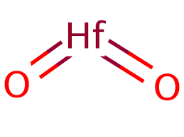 Try hafnium oxide. Back in 2007, IBM and Intel announced that they would begin producing the next-generation computer chips that were smaller and faster than silicon by using hafnium oxide.
Hafnium oxide is a stable, inorganic compound that is a much more effective dielectric than silicon. According to Paul McIntyre from the Stanford University Engineering and Science Institute, California, “Researchers have learnt to deposit very thin films of hafnium oxide and mix it with silica or silicon nitride at the molecular scale to tailor their insulating and charge storage properties.” In addition to replacing silicon in transistors, in 2012, scientists at the University of Cambridge developed a manufacturing process that created hafnium oxide that has the benefit of being a room-temperature, high-deposition rate process. This makes the deployment of hafnium oxide-based electronics, which includes solar cells and semiconductors, along with microchips, much more efficient. The rapid pace of electric development has required the industry to move away from silicon to make its ever-shrinking capacitors. Hafnium oxide is a stepping stone towards more innovation, ensuring the future progress of faster, smarter computers. For more information, please visit https://www.sputtertargets.net/. LOW-E glass is a kind of processed glass products coated with a spectrally functional film made by sputtering to achieve transparent light-transmissive. These films are selective with high reflection to infrared light and no reflection on visible light. Low-E films are made by physical vapor deposition, and the sputtering target is the source material. Under normal circumstances, the energy-saving performance of the ordinary uncoated three-glass two-chamber insulating glass is not as good as that of the single-chamber insulating glass using Low-E coated glass. LOW-E glass can be divided into online and offline Low-E coated glass according to the processing method. Therefore, Low-E coated glass plays a vital role in residential glass door and window applications. 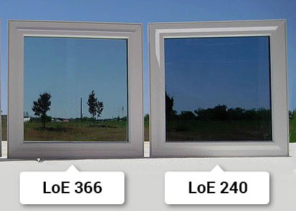 1. What is Low-E glass?
|

 RSS订阅
RSS订阅
