|
Tungsten sputtering targets are the unsung heroes of the electronics and semiconductor industries, enabling the production of cutting-edge devices that power our modern world. These targets play a crucial role in the thin film deposition process, a fundamental technique in semiconductor manufacturing, OLED production, and more. But what goes into making these high-purity tungsten sputtering targets, and why are they so essential? Let's take a closer look behind the scenes. The Quest for Purity Tungsten, a heavy and dense metal with exceptional thermal and electrical conductivity properties, is the material of choice for sputtering targets. However, not all tungsten is created equal. The semiconductor and electronics industries demand the highest levels of purity to ensure the reliability and performance of their devices. The manufacturing process begins with sourcing raw tungsten materials, typically in the form of tungsten oxides or powders. These raw materials undergo a series of complex chemical and metallurgical processes to extract and refine the tungsten into high-purity metal. Impurities, even in trace amounts, can significantly impact the quality of the sputtering process and the final product. 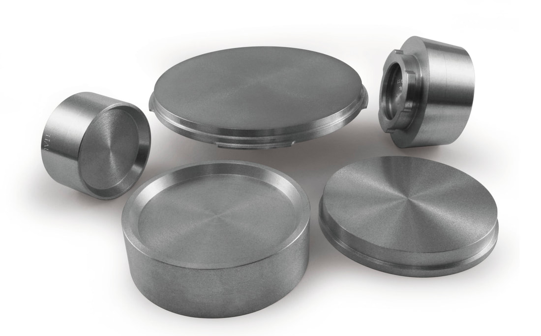 Powder Metallurgy and Forming
Once the tungsten metal achieves the required level of purity, it is transformed into sputtering targets through a process known as powder metallurgy. In this process, the tungsten powder is carefully blended with a binding agent to create a homogenous mixture. This mixture is then pressed into the desired shape, typically a cylindrical or planar target. The pressing stage is critical for achieving the right density and uniformity. The formed targets must have a precise thickness, ensuring even sputtering during the deposition process. Achieving this level of precision requires expertise and state-of-the-art equipment. Sintering and Thermal Treatment After forming, the tungsten targets undergo sintering, a high-temperature process that fuses the tungsten particles together. This step enhances the mechanical strength of the target and further eliminates any remaining impurities. Sintering can occur in a vacuum or hydrogen atmosphere to prevent contamination. Following sintering, the targets may undergo additional thermal treatments to optimize their microstructure. These treatments help ensure the targets can withstand the rigorous conditions of the sputtering process, which involves bombarding the target material with high-energy ions to dislodge atoms for deposition onto substrates. Quality Control and Testing Quality control is paramount throughout the manufacturing process. Advanced techniques such as X-ray diffraction and spectroscopy are employed to analyze the target's composition and crystal structure. These tests ensure that the final product meets the stringent purity and quality standards required by the semiconductor and electronics industries. Customization and Innovation While the basics of tungsten sputtering target manufacturing remain consistent, innovation continues to drive the industry forward. Research and development efforts focus on refining the manufacturing processes, exploring new materials and coatings, and optimizing target designs to enhance performance and longevity. Conclusion Tungsten sputtering targets are a testament to precision engineering and materials science. Behind the scenes, these high-purity targets undergo a rigorous journey from raw materials to the finished product, with each step carefully controlled and monitored. Their exceptional purity, density, and uniformity make them indispensable tools in the production of semiconductor devices, OLED screens, and a wide range of other electronic components. As technology continues to advance, the manufacturing of tungsten sputtering targets will undoubtedly play a pivotal role in shaping the future of electronics and semiconductor industries. For more information, please visit sputtertargets.net.
0 评论
写评论。 |
 RSS订阅
RSS订阅
